| New version of the Haynes-Shockley experiment |

|
|
The
experiment proposed in 1949 by J.R.Haynes and W.Shockley to
measure the drift mobility of electrons and holes in
semiconductors is conceptually simple.
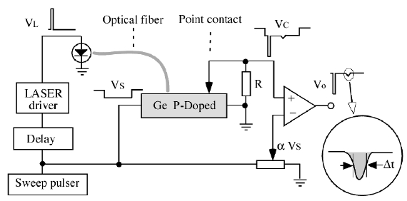
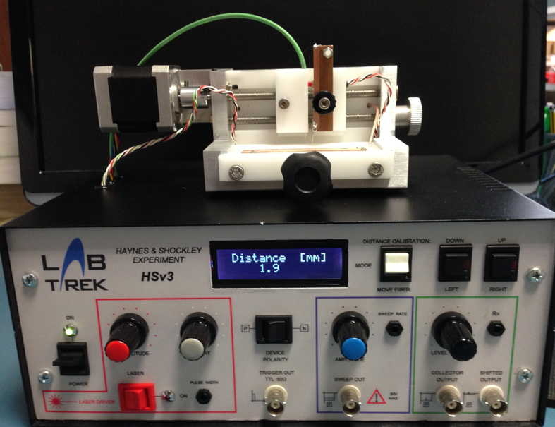
The main difficulties are in the sample preparation, in the charge injection and in the signal detection. It is an experiment with great educational value, because it allows direct investigation of the drift velocity, of the diffusion process and of the recombination of excess charge carriers. In our new setup the excess carriers are optically injected (using internal photoelectric effect) avoiding the need of a reliable point-contact emitter. 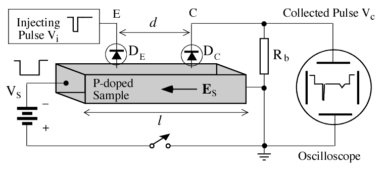 Figure 1 : Setup of the original H-S apparatus The
block diagram of the original Haynes and Shockely
experiment is shown in Fig.1.
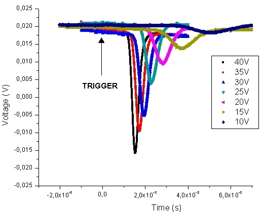
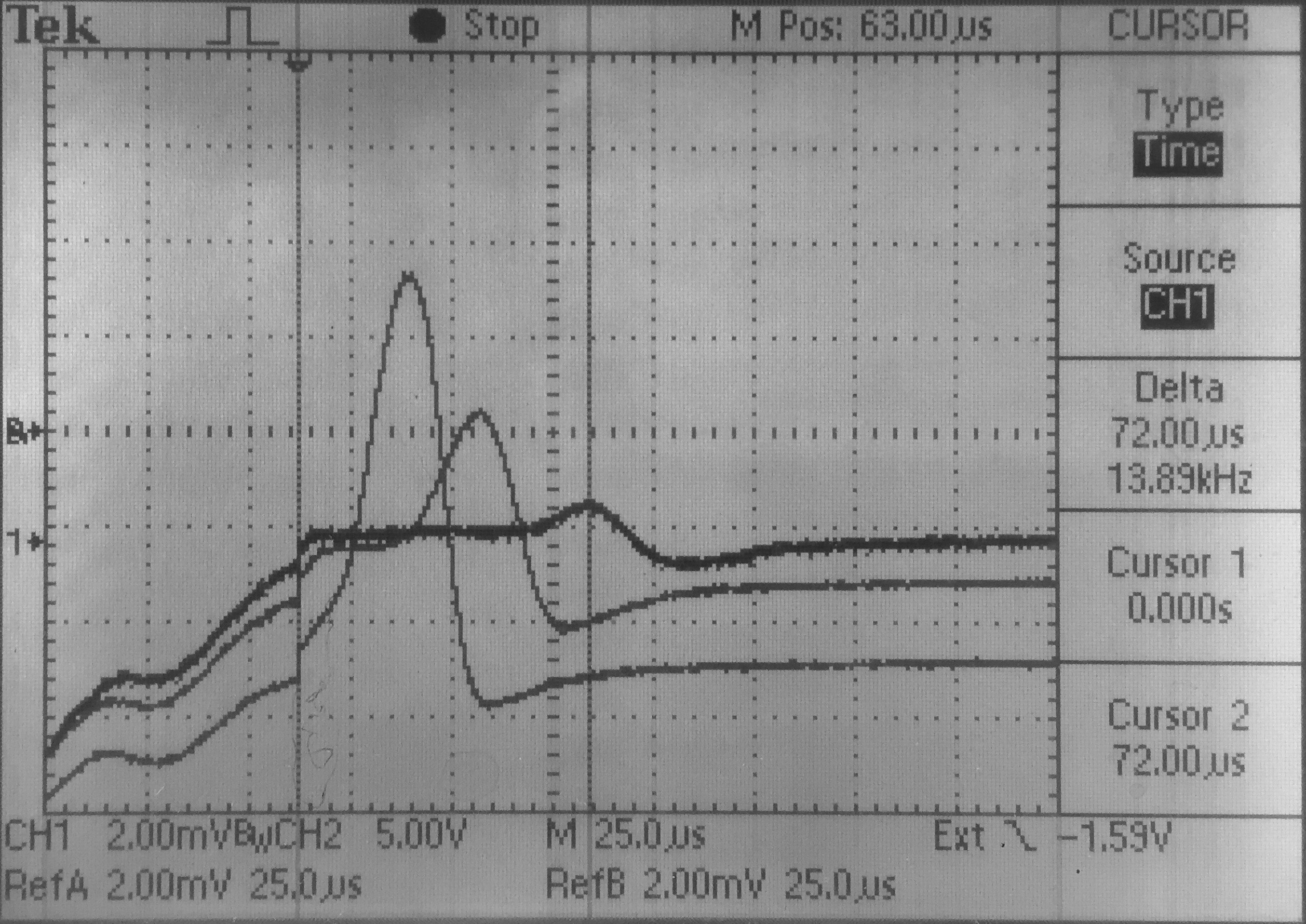
As an example, let us consider a P-doped semiconductor bar, of length l, with ohmic contacts soldered at both ends Inside the sample an electric field (named sweep field Es) is temporarily produced by a pulsed generator, sketched in Figure 1 as a battery in series with a switch. Two point contacts (electrodes E and C) are made by two metal needled separated by a distance d . The point contacts are (partially) rectifying and therefore they are drawn as diodes in figure 1 By applying to the electrode E (emitter) a short negative pulse voltage with an amplitude large enough to forward bias the diode DE, electrons will be injected into the crystal region underlying the emitter. This electron pulse will drift, under the electric field action, with velocity vd, and after some time t it will reach the region underlying the electrode C (collector). When the excess electron pulse reaches the point contact C, the minority charge carrier density is locally increased, thus increasing the inverse current and producing a voltage drop across the resistance R. On the oscilloscope screen we may observe a first short negative pulse, with amplitude comparable to that of the injection pulse and, after some delay t, a second negative pulse, wider and much smaller than the first one. The first peak is simultaneous with the injection pulse: it is due to the electromagnetic signal propagating across the sample (at the light speed). The second pulse corresponds to the excess electon distribution passing under the collector contact: its shape is approximately gaussian and its amplitude and width are determined by diffusion and recombination processes. The actual pulse shape depends on the drift time t, on the covered distance d , on the drift velocity μEs, where μ is the electron mobility , and also on the diffusion constant D. The injected electrons in fact, while drifting towards the collector, diffuse broadening their spatial distribution, so that the width of the collected pulse increases with the time of flight t. Moreover the electrons recombine with holes so that their number decreases exponentially with time t as: N(t) = No exp (-t/τ) where τ is the lifetime of the excess charge carriers.
The measurement of the time of flight t. and of the distance d between the fiber and the point contact gives the drift velocity vd: vd = d/t . The measurements of the amplitude VS of the sweep pulse and of the sample length l give the value of the sweep field ES =VS/l and therefore of the electron mobility μ : μ = vd/Es = (d l)/(t VS). The measurement of the pulse width at half-height Δt gives the diffusion constant D.The diffusion produces in fact a gaussian broadening of the injected narrow peak, resulting in a pulse width at half-height Δx=sqrt(16 ln2 Dt) that drifts with a velocity vd : it takes therefore the time Δt=Δx/vd to cross the collector position . The ratio D/μ obeys to the Einstein relation: D/μ=kT/e=0.026 volt at T=300 K. In a semi logarithmic plot of the collected pulse areas versus time, the slope gives the reciprocal of the the recombination lifetime τ. P-doped
Ge sample
 I-V of the point-contact diode Electron pulse for different distances N-doped Ge sample 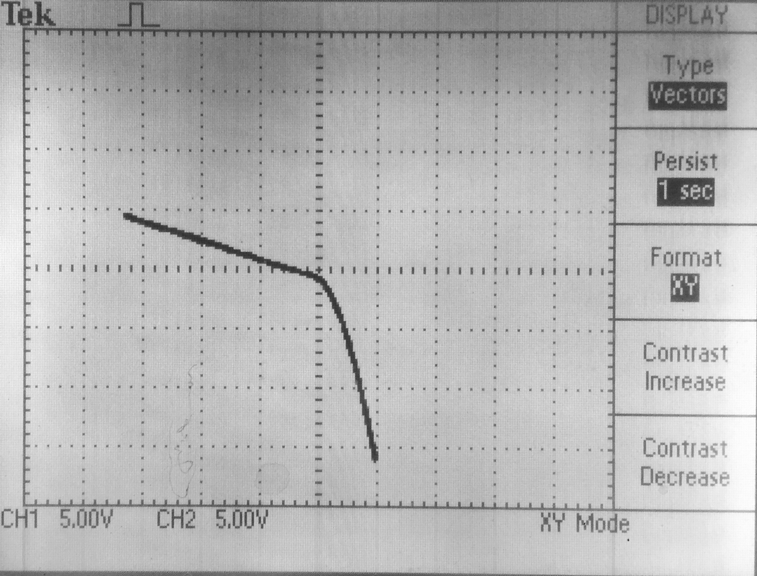
 I-V of the point-contact diode Hole pulse for different distances Ref.: An improved version of the Haynes-Shockley experiment Am. J. Phys. 68, 80 (2000) |
|
 Possible measurements:
The Haynes-Shockley experiment requires (not included):
Java Applets simulations of the Haynes-Shockley signal :
|